Using Proteus for PCB Design: Step-by-Step Guide
Proteus is one of the most versatile tools for PCB design, offering a seamless experience for creating schematics, laying out PCBs, and preparing designs for manufacturing. Its intuitive features make it a favorite among engineers, students, and hobbyists.
This guide will show you how to design PCB in Proteus step by step. By the end, you’ll have a complete understanding of creating a schematic, transitioning to PCB layout, and generating files for manufacturing. Let’s dive into this comprehensive Proteus PCB tutorial!

Setting Up a New Project in Proteus
Step 1: Launching the New Project Wizard
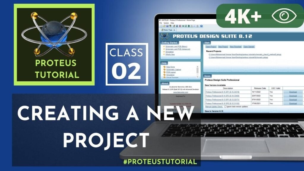
- Open Proteus and select the “New Project Wizard” from the welcome screen.
- Enter a project name and choose a directory to save the project files.
- Decide the type of project:
- Schematic only
- PCB layout only
- Both schematic and PCB layout
Pro Tip: Save frequently and organize your projects in separate folders to avoid confusion during future edits.
Step 2: Using Templates
- For beginners, stick to the default templates provided by Proteus for schematic and PCB layouts.
- Advanced users can create custom templates by setting preferred grid sizes, layer configurations, or design styles.
Learn More: Check Proteus documentation to customize templates for your specific needs.
Designing the Schematic
The schematic forms the backbone of your PCB design. Here’s how to create it effectively:
Step 1: Adding Components
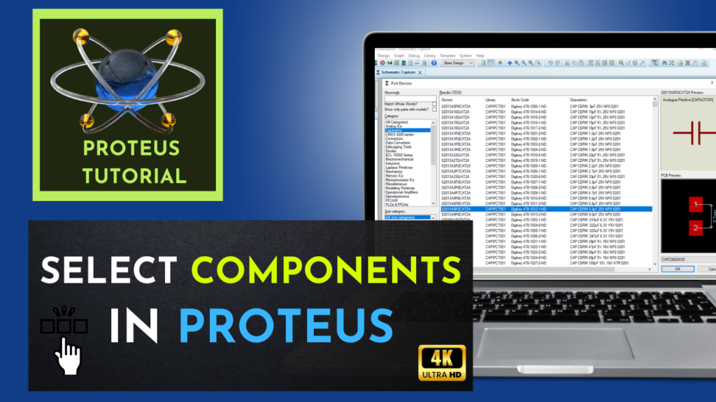
- Open the Library Picker and search for components using keywords.
- Example: Search for “LM358” to find an operational amplifier.
- Double-click to add selected components to the Parts Bin.
- Repeat the process for connectors, resistors, and capacitors. Use values or packaging as keywords (e.g., “10uF 0805” for a capacitor).
Step 2: Placing Components
- Drag components from the parts bin onto the schematic workspace.
- Rotate components as needed using the plus (+) and minus (-) keys.
Tip: Keep your schematic clean by aligning components neatly. Use grid snapping for uniform placement.
Step 3: Wiring Components
- Switch to Wire Mode from the toolbar.
- Click between component pins to draw connections. Proteus will automatically generate nets for connected pins.
- Add power (VCC) and ground (GND) terminals using the Terminal Mode.
- Name terminals for clarity. For example, label VCC and GND to match the power supply.
Pro Tip: Label critical nets (like signals or clocks) for better readability and error detection in the PCB layout phase.
Step 4: Adding Design Annotations
- Assign unique designators to each component (e.g., R1, C1).
- Verify connections using the Design Rule Check (DRC) to ensure there are no errors.
Switching to PCB Layout
Once your schematic is complete, transition seamlessly to the PCB layout.
Step 1: Setting the Board Edge
- Select the 2D Graphics Tool and ensure the layer is set to “Board Edge.”
- Draw the board outline using the mouse, with precise dimensions based on your enclosure or application needs.
Example: For a compact IoT device, you might draw a 50mm x 50mm square.
Step 2: Placing Components
- Components from your schematic will appear in the PCB Bin with references (e.g., R1, U1).
- Drag components onto the board and arrange them logically.
- Example: Place high-current components like power regulators close to connectors.
- Use green rat-nest lines as guides for connections.
Step 3: Configuring Design Rules
- Open the Design Rule Manager from the Technology Menu.
- Set trace widths, clearances, and via sizes. Adjust these based on manufacturing capabilities:
- Trace width: 10mil for standard signals, 30mil+ for power traces.
- Clearance: 10mil for signal traces.
Routing the PCB
Routing is one of the most critical steps in PCB design. Proteus offers manual and automatic options.
Manual Routing
- Select Track Mode and choose the starting layer (e.g., Top Layer).
- Click on a pad to begin routing and drag to the destination pad.
- Use shortcuts for efficiency:
- Spacebar: Insert via and switch layers.
- Left-click: Anchor a point or change direction.
Auto Routing
- Use the auto-router for quicker routing.
- Customize auto-routing settings to prioritize critical nets.
Reviewing and Finalizing the PCB Design
Step 1: Design Rule Check (DRC)
Run the DRC to detect and fix issues like unconnected nets or overlapping traces.
Step 2: Exporting Files
- Generate Gerber files for PCB fabrication.
- Export ODB++ files if required by your manufacturer.
Pro Tip: Always review exported files in a Gerber viewer to catch potential errors.
Advanced Features in Proteus
3D Models
- Import STEP files for components to visualize the PCB in 3D.
- Use the 3D viewer to inspect solder masks and alignment with enclosures.
Exporting to MCAD
Export your design to MCAD tools for enclosure design or simulations. Proteus supports industry-standard file formats for seamless integration.
Common Issues and Troubleshooting in Proteus
Problem: Incorrect Connections
Solution: Use the DRC tool to highlight unconnected nets and fix them in the schematic.
Problem: Overlapping Components
Solution: Adjust placement using the snap-to-grid feature for alignment.
Conclusion
Proteus simplifies PCB design with its robust features and intuitive workflows. From schematic design to routing and exporting, every step is designed to ensure your PCB is production-ready. Follow this guide to design PCB in Proteus efficiently and confidently.
For more insights and advanced Proteus PCB tutorials, explore our other guides!


